Zen 3
Zen 3 is the codename for a CPU microarchitecture by AMD, released on November 5, 2020.[1][2] It is the successor to Zen 2 and uses TSMC's 7 nm process for the chiplets and GlobalFoundries's 14 nm process for the I/O die on the server chips and 12 nm for desktop chips.[3] Zen 3 powers Ryzen 5000 mainstream desktop processors (codenamed "Vermeer") and Epyc server processors (codenamed "Milan").[4][5] Zen 3 is supported on motherboards with 500 series chipsets; 400 series boards also saw support on select B450 / X470 motherboards with certain BIOSes.[6] Zen 3 is expected to be the last microarchitecture before AMD switches to DDR5 memory and new sockets.[2] According to AMD, Zen 3 has a 19% higher instructions per cycle (IPC) on average than Zen 2.
 | |
| General information | |
|---|---|
| Launched | November 5, 2020 |
| Designed by | AMD |
| Common manufacturer(s) | |
| Cache | |
| L1 cache | 64 KB per core |
| L2 cache | 512 KB per core |
| L3 cache | 32 MB per CCX |
| Architecture and classification | |
| Technology node | TSMC 7 nm |
| Physical specifications | |
| Cores |
|
| Package(s) |
|
| Socket(s) | |
| Products, models, variants | |
| Product code name(s) |
|
| History | |
| Predecessor | Zen 2 |
Features
Zen 3 is a significant incremental improvement over its predecessors, with an IPC increase of 19%,[7] and being capable of reaching higher clock speeds.
Like Zen 2, Zen 3 is composed of up to 2 core complex dies (CCD) along with a separate IO die containing the I/O components. A Zen 3 CCD is composed of a single core complex (CCX) containing 8 CPU cores and 32 MB of shared L3 cache, this is in contrast to Zen 2 where each CCD is composed of 2 CCX, each containing 4 cores each as well as 16 MB of L3 cache. The new configuration allows all 8 cores of the CCX to directly communicate with each other and the L3 Cache instead of having to use the IO die through the Infinity Fabric.[7]
Zen 3 (along with AMD's RDNA2 GPUs) were also the first implementation of Resizable BAR, an optional feature introduced in PCIe 2.0, that was branded as Smart Access Memory (SAM). This technology allows CPU to directly access all of compatible video card's VRAM.[8] Intel and Nvidia have since implemented this feature as well.[9]
%2540Zen3%2540Vermeer%2540Ryzen_5_5600X%2540100-000000064_BG_2042SUS_9JF6228V00014_DSCx2.jpg.webp) A de-lidded Ryzen 5 5600X. Only one CCD is present. The contacts for a second CCD are visible.
A de-lidded Ryzen 5 5600X. Only one CCD is present. The contacts for a second CCD are visible.%2540Zen3%2540Vermeer%2540Ryzen_5_5600X%2540100-000000064_BG_2042SUS_9JF6228V00014_DSCx4%2540IR.jpg.webp) Close-up of the CCD, taken under infrared lighting. This die was damaged by the de-lidding process.
Close-up of the CCD, taken under infrared lighting. This die was damaged by the de-lidding process.%2540Zen3%2540Vermeer%2540Ryzen_5_5600X%2540100-000000064_BG_2042SUS_9JF6228V00014_DSCx3%2540IR.jpg.webp) Close-up of the I/O die
Close-up of the I/O die
In Zen 3, a single 32MB L3 cache pool is shared among all 8 cores in a chiplet, vs Zen 2's two 16MB pools each shared among 4 cores in a core complex, of which there were two per chiplet. This new arrangement improves the cache hit rate as well as performance in situations that require cache data to be exchanged among cores, but increases cache latency from 39 cycles in Zen 2 to 46 clock cycles and halves per-core cache bandwidth, although both problems are partially mitigated by higher clock speeds. Total cache bandwidth on all 8 cores combined remains the same due to power consumption concerns. L2 cache capacity and latency remain the same at 512KB and 12 cycles. All cache read and write operations are done at 32 bytes per cycle.[10]
Improvements
Zen 3 has made the following improvements over Zen 2:[10][11]
- An increase of 19% in instructions per clock
- The base core chiplet has a single eight-core complex (versus two four-core complexes in Zen 2)
- A unified 32MB L3 cache pool equally available to all 8 cores in a chiplet, vs Zen 2's two 16MB pools each shared among 4 cores in a core complex.
- On mobile: A unified 16MB L3
- A unified 8-core CCX (from 2x 4-Core CCX per CCD)
- Increased branch prediction bandwidth. L1 branch target buffer size increased to 1024 entries (vs 512 in Zen 2)
- New Instructions
- VAES - 256-bit Vector AES instructions
- INVLPGB - Broadcast TLB flushing
- CET_SS - Control-flow Enforcement Technology / Shadow Stack
- Improved integer units
- 96 entry integer scheduler (up from 92)
- 192 entry physical register file (up from 180)
- 10 issue per cycle (up from 7)
- 256 entry reorder-buffer (up from 224)
- fewer cycles for DIV/IDIV ops (10...20 from 16...46)
- Improved floating point units
- 6 µOP dispatch width (up from 4)
- FMA latency reduced by 1 cycle (down from 5 to 4)
Feature tables
CPUs
CPU features table
APUs
APU features table
Products
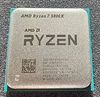
On October 8, 2020, AMD announced four Zen 3-based desktop Ryzen processors, consisting of one Ryzen 5, one Ryzen 7, and two Ryzen 9 CPUs and featuring between 6 and 16 cores.[1]
Vermeer
| Model | Release date and price |
Fab | Chiplets | Cores (threads) |
Core config[lower-roman 1] | Clock rate (GHz) | Cache | Socket | PCIe lanes |
Memory support |
TDP | |||
|---|---|---|---|---|---|---|---|---|---|---|---|---|---|---|
| Base | Boost | L1 | L2 | L3 | ||||||||||
| Mainstream | ||||||||||||||
| Ryzen 5 5600X[12] | November 5, 2020 US $299 |
TSMC 7FF |
1 × CCD 1 × I/O |
6 (12) | 1 × 6 | 3.7 | 4.6 | 32 KB inst. 32 KB data per core |
512 KB per core |
32 MB per CCX |
AM4 | 24 | DDR4-3200 dual-channel |
65 W |
| Performance | ||||||||||||||
| Ryzen 7 5800[13] | January 12, 2021 OEM |
TSMC 7FF |
1 × CCD 1 × I/O |
8 (16) | 1 × 8 | 3.4 | 4.6 | 32 KB inst. 32 KB data per core |
512 KB per core |
32 MB per CCX |
AM4 | 24 | DDR4-3200 dual-channel |
65 W |
| Ryzen 7 5800X[14] | November 5, 2020 US $449 |
3.8 | 4.7 | 105 W | ||||||||||
| Enthusiast | ||||||||||||||
| Ryzen 9 5900[15] | January 12, 2021 OEM |
TSMC 7FF |
2 × CCD 1 × I/O |
12 (24) | 2 × 6 | 3.0 | 4.7 | 32 KB inst. 32 KB data per core |
512 KB per core |
64 MB 32 MB per CCX |
AM4 | 24 | DDR4-3200 dual-channel |
65 W |
| Ryzen 9 5900X[16] | November 5, 2020 US $549 |
3.7 | 4.8 | 105 W | ||||||||||
| Ryzen 9 5950X[17] | November 5, 2020 US $799 |
16 (32) | 2 × 8 | 3.4 | 4.9 | |||||||||
- Core Complexes (CCX) × cores per CCX
Cezanne
| Model | Release date & price |
Fab | CPU | GPU | Memory support | TDP | |||||||||
|---|---|---|---|---|---|---|---|---|---|---|---|---|---|---|---|
| Cores (threads) |
Core config[lower-roman 1] | Clock rate (GHz) | Cache | Architecture | Config[lower-roman 2] | Clock | Processing power (GFLOPS)[lower-roman 3] | ||||||||
| Base | Boost | L1 | L2 | L3 | |||||||||||
| Ryzen 3 5300GE[note 1][18] | 13 April 2021[19] OEM |
TSMC 7FF |
4 (8) | 1 × 4 | 3.6 | 4.2 | 32 KB inst. 32 KB data per core |
512 KB per core |
8 MB | GCN 5th gen | 384:24:8 6 CU |
1700 MHz | 1305.6 | DDR4-3200 dual-channel |
35 W |
| Ryzen 3 5300G[note 1][20] | 4.0 | 65 W | |||||||||||||
| Ryzen 5 5600GE[note 1][21] | 6 (12) | 1 × 6 | 3.4 | 4.4 | 16 MB | 448:28:8 7 CU |
1900 MHz | 1702.4 | 35 W | ||||||
| Ryzen 5 5600G[note 1][22] | 13 April 2021[19] OEM 5 August 2021 US $259[23] |
3.9 | 65 W | ||||||||||||
| Ryzen 7 5700GE[note 1][24] | 13 April 2021[19] OEM |
8 (16) | 1 × 8 | 3.2 | 4.6 | 512:32:8 8 CU |
2000 MHz | 2048 | 35 W | ||||||
| Ryzen 7 5700G[note 1][25] | 13 April 2021[19] OEM 5 August 2021 US $359[23] |
3.8 | 65 W | ||||||||||||
- Core Complexes (CCX) × cores per CCX
- Unified shaders : texture mapping units : render output units and compute units (CU)
- Single precision performance is calculated from the base (or boost) core clock speed based on a FMA operation.
- Model also available as PRO version[note 2][note 3][note 4][note 5][note 6][note 7], released 1 June 2021[note 8].
- "AMD Ryzen™ 3 PRO 5350GE". AMD.
- "AMD Ryzen™ 3 PRO 5350G". AMD.
- "AMD Ryzen™ 5 PRO 5650GE". AMD.
- "AMD Ryzen™ 5 PRO 5650G". AMD.
- "AMD Ryzen™ 7 PRO 5750GE". AMD.
- "AMD Ryzen™ 7 PRO 5750G". AMD.
- "AMD Announces Ryzen 5000G and PRO 5000G Desktop Processors". TechPowerUp. June 1, 2021.
Cezanne
| Model | Release date |
Fab | CPU | GPU | Socket | PCIe lanes |
Memory support | TDP | |||||||||
|---|---|---|---|---|---|---|---|---|---|---|---|---|---|---|---|---|---|
| Cores (threads) |
Core config[lower-roman 1] | Clock rate (GHz) | Cache | Architecture | Config[lower-roman 2] | Clock | Processing power (GFLOPS)[lower-roman 3] | ||||||||||
| Base | Boost | L1 | L2 | L3 | |||||||||||||
| Ryzen 3 5400U[note 1][26][27] | January 12, 2021 | TSMC 7FF |
4 (8) | 1 × 4 | 2.6 | 4.0 | 32 KB inst. 32 KB data per core |
512 KB per core |
8 MB | GCN 5th gen | 320:20:8 6 CU |
1600 MHz | 1228.8 | FP6 | 16 (8+4+4) PCIe 3.0 |
DDR4-3200 LPDDR4-4266 dual-channel |
10–25 W |
| Ryzen 5 5600U[note 1][28] | 6 (12) | 1 × 6 | 2.3 | 4.2 | 16 MB | 320:20:8 7 CU |
1800 MHz | 1612.8 | 10-25 W | ||||||||
| Ryzen 5 5600H[29][30] | 3.3 | 35–54 W | |||||||||||||||
| Ryzen 5 5600HS[31] | 3.0 | 35 W | |||||||||||||||
| Ryzen 7 5800U[note 1][32] | 8 (16) | 1 × 8 | 1.9 | 4.4 | 320:20:8 8 CU |
2000 MHz | 2048 | 10–25 W | |||||||||
| Ryzen 7 5800H[33][34] | 3.2 | 35–54 W | |||||||||||||||
| Ryzen 7 5800HS[35] | 2.8 | 35 W | |||||||||||||||
| Ryzen 9 5900HS[36] | 3.0 | 4.6 | 2100 MHz | 2150.4 | |||||||||||||
| Ryzen 9 5900HX[37] | 3.3 | 35–54 W | |||||||||||||||
| Ryzen 9 5980HS[38] | 3.0 | 4.8 | 35 W | ||||||||||||||
| Ryzen 9 5980HX[39] | 3.3 | 35–54 W | |||||||||||||||
- Core Complexes (CCX) × cores per CCX
- Unified shaders : texture mapping units : render output units and compute units (CU)
- Single precision performance is calculated from the base (or boost) core clock speed based on a FMA operation.
- Model also available as PRO version[note 2][note 3][note 4], released on March 16, 2021.
- "AMD Ryzen™ 3 PRO 5450U". AMD.
- "AMD Ryzen™ 5 PRO 5650U". AMD.
- "AMD Ryzen™ 7 PRO 5850U". AMD.
Epyc microprocessors
The Epyc server line of chips based on Zen 3 is named Milan and is the final generation of chips using the SP3 socket.[5] Epyc Milan was released on March 15, 2021.[40]
| Model | Price | Fab | Chiplets | Cores (threads) |
Core config[lower-roman 1] | Clock rate (GHz) | Cache | Socket & configuration |
TDP | |||
|---|---|---|---|---|---|---|---|---|---|---|---|---|
| Base | Boost | L1 | L2 | L3 | ||||||||
| EPYC 7763 | US $7890 | 7 nm | 8 × CCD 1 × I/O |
64 (128) | 8 × 8 | 2.45 | 3.50 | 32 KB inst. 32 KB data per core |
512 KB per core |
256 MB 32 MB per CCX |
SP3 2P |
280 W |
| EPYC 7713 | US $7060 | 2.00 | 3.675 | 225 W | ||||||||
| EPYC 7713P | US $5010 | SP3 1P | ||||||||||
| EPYC 7663 | US $6366 | 56 (112) | 8 × 7 | 2.00 | 3.50 | SP3 2P |
240 W | |||||
| EPYC 7643 | US $4995 | 48 (96) | 8 × 6 | 2.30 | 3.60 | 225 W | ||||||
| EPYC 75F3 | US $4860 | 32 (64) | 8 × 4 | 2.95 | 4.00 | 280 W | ||||||
| EPYC 7543 | US $3761 | 2.80 | 3.70 | 225 W | ||||||||
| EPYC 7543P | US $2730 | SP3 1P | ||||||||||
| EPYC 7513 | US $2840 | 2.60 | 3.65 | 128 MB 16 MB per CCX |
SP3 2P |
200 W | ||||||
| EPYC 7453 | US $1570 | 4 × CCD 1 × I/O |
28 (56) | 4 × 7 | 2.75 | 3.45 | 64 MB 16 MB per CCX |
225 W | ||||
| EPYC 74F3 | US $2900 | 8 × CCD 1 × I/O |
24 (48) | 8 × 3 | 3.20 | 4.00 | 256 MB 32 MB per CCX |
240 W | ||||
| EPYC 7443 | US $2010 | 4 × CCD 1 × I/O |
4 × 6 | 2.85 | 4.00 | 128 MB 32 MB per CCX |
200 W | |||||
| EPYC 7443P | US $1337 | SP3 1P | ||||||||||
| EPYC 7413 | US $1825 | 2.65 | 3.60 | SP3 2P |
180 W | |||||||
| EPYC 73F3 | US $3521 | 8 × CCD 1 × I/O |
16 (32) | 8 × 2 | 3.50 | 4.00 | 256 MB 32 MB per CCX |
240 W | ||||
| EPYC 7343 | US $1565 | 4 × CCD 1 × I/O |
4 × 4 | 3.20 | 3.90 | 128 MB 32 MB per CCX |
190 W | |||||
| EPYC 7313 | US $1083 | 3.00 | 3.70 | 155 W | ||||||||
| EPYC 7313P | US $913 | SP3 1P | ||||||||||
| EPYC 72F3 | US $2468 | 8 × CCD 1 × I/O |
8 (16) | 8 × 1 | 3.70 | 4.10 | 256 MB 32 MB per CCX |
SP3 2P |
180 W | |||
- Core Complexes (CCX) × cores per CCX
References
- Su, Lisa (October 8, 2020). Where Gaming Begins, AMD Ryzen™ Desktop Processors.
- Joel Hruska (January 10, 2020). "AMD's Lisa Su Confirms Zen 3 Coming in 2020, Talks Challenges in Notebooks". ExtremeTech.
- Dr. Ian Cutress (October 9, 2020). "AMD Ryzen 5000 and Zen 3 on Nov 5th: +19% IPC, Claims Best Gaming CPU". AnandTech.
- Mark Knapp (October 8, 2020). "AMD Zen 3 release date, specs and price: everything we know about AMD Ryzen 5000". TechRadar.
- Alcorn, Paul (October 5, 2019). "AMD dishes on Zen 3 and Zen 4 architecture, Milan and Genoa roadmap". Tom's Hardware. Retrieved October 5, 2019.
- Hruska, Joel (May 20, 2020). "AMD Will Support Zen 3, Ryzen 4000 CPUs on X470, B450 Motherboards". ExtremeTech. Retrieved May 20, 2020.
- "AMD "Zen 3" Core Architecture". AMD. Retrieved November 8, 2020.
- Alcorn, Paul (November 6, 2020). "AMD Zen 3 Ryzen 5000 Price, Specs, Release Date, Performance, All We Know". Tom's Hardware. Retrieved November 8, 2020.
- "GeForce RTX 30 Series Performance Accelerates With Resizable BAR Support | GeForce News". NVIDIA. Retrieved August 13, 2021.
- Cutress, Ian; Frumusanu, Andrei (November 5, 2020). "AMD Zen 3 Ryzen Deep Dive Review: 5950X, 5900X, 5800X and 5600X Tested". www.anandtech.com. Retrieved December 7, 2020.
- Alcorn, Paul (November 26, 2020). "AMD Ryzen 9 5950X and 5900X Review: Zen 3 Breaks the 5 GHz Barrier". Tom's Hardware. Retrieved December 25, 2020.
- "AMD Ryzen 5 5600X Desktop Processor". AMD.
- "AMD Ryzen 7 5800". AMD.
- "AMD Ryzen 7 5800X Desktop Processor". AMD.
- "AMD Ryzen 9 5900". AMD.
- "AMD Ryzen 9 5900X Desktop Processor". AMD.
- "AMD Ryzen 9 5950X Desktop Processor". AMD.
- "AMD Ryzen 3 5300GE". AMD.
- "AMD Ryzen 5000G APUs: OEM Only For Now, Full Release Later This Year". AnandTech. April 13, 2021.
- "AMD Ryzen 3 5300G". AMD.
- "AMD Ryzen 5 5600GE". AMD.
- "AMD Ryzen 5 5600G". AMD.
- "AMD Ryzen 5000G: Zen 3 APUs for Desktop Coming August 5th". AnandTech.
- "AMD Ryzen 7 5700GE". AMD.
- "AMD Ryzen 7 5700G". AMD.
- "AMD Ryzen™ 3 5400U". AMD.
- "AMD Ryzen 3 5400U Mobile processor - 100-000000288". www.cpu-world.com. Retrieved September 17, 2021.
- "AMD Ryzen™ 5 5600U". AMD.
- "AMD Ryzen™ 5 5600H". AMD.
- "AMD Ryzen 5 5600H Mobile processor - 100-000000296". www.cpu-world.com. Retrieved September 17, 2021.
- "AMD Ryzen™ 5 5600HS". AMD.
- "AMD Ryzen™ 7 5800U". AMD.
- "AMD Ryzen™ 7 5800H". AMD.
- "AMD Ryzen 7 5800H Specs". TechPowerUp. Retrieved September 17, 2021.
- "AMD Ryzen™ 7 5800HS". AMD.
- "AMD Ryzen™ 9 5900HS". AMD.
- "AMD Ryzen™ 9 5900HX". AMD.
- "AMD Ryzen™ 9 5980HS". AMD.
- "AMD Ryzen™ 9 5980HX". AMD.
- Alcorn, Paul (March 15, 2021). "Watch AMD's EPYC 7003 Milan Launch Here". Tom's Hardware. Retrieved July 23, 2021.